Introduction
When starting electronics projects, most makers begin by testing circuits on a breadboard. But breadboards are messy, unreliable, and not suitable for long‑term use.
That’s where PCBs (Printed Circuit Boards) come in.
A PCB is the professional, permanent way to connect components with neat copper tracks instead of wires.
In this beginner’s guide, you’ll learn:
- What a PCB is and why it matters.
- Steps in designing your first PCB.
- Two free beginner‑friendly tools: EasyEDA (online) & KiCad (desktop, open-source).
What is a PCB (Printed Circuit Board)?
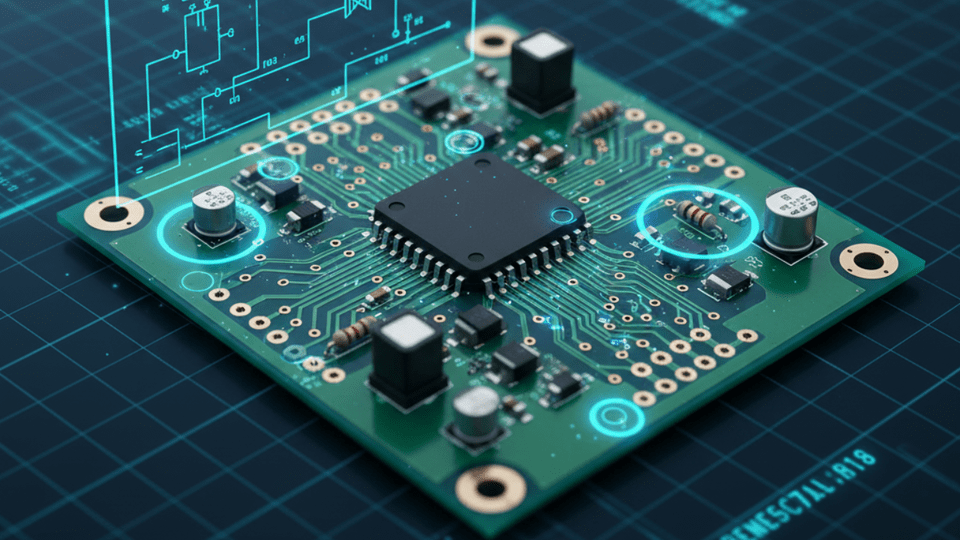
A PCB is a board made of non‑conductive material (fiberglass), with copper tracks etched on it that act as the “wiring” for your circuit.
- Single‑layer PCB: Copper on one side (basic).
- Double‑layer PCB: Copper on both sides (common).
- Multi‑layer PCB: 4, 6, or more layers for complex circuits.
Instead of tangled wires → PCBs make projects compact, professional, and reliable.
Why Learn PCB Design?
- Makes your DIY robot/sensor projects permanent.
- Prepares you for professional electronics careers.
- Easy and free tools mean you can design PCBs without being an engineer.
- Manufacturers like JLCPCB, PCBWay deliver your design in <1 week!
Steps to Design a PCB (General Workflow)
- Schematic Design
- Draw your circuit diagram digitally.
- Add components (resistors, ICs, Arduino header, etc.).
- Connect with “wires” (nets).
- PCB Layout
- Place actual footprints of components on a board outline.
- Route copper tracks (auto‑route or manual).
- Define power/ground planes.
- Check Design Rules (DRC)
- Ensure no overlaps or errors.
- Generate Gerber Files
- Universal file format for PCB manufacturers.
- Order PCB Fabrication 🏭
- Upload Gerber files to JLCPCB/PCBWay/EasyEDA.
- Select thickness, color, finish.
Beginner Tools for PCB Design
- EasyEDA (Online Tool) ✨
- Free, web‑based, no installation.
- Perfect for beginners → intuitive drag & drop interface.
- Built‑in library of components.
- Direct integration with JLCPCB → one‑click ordering.
- Bonus: Simulation support.
Quick Tutorial (EasyEDA):
- Sign up at easyeda.com.
- Click New Project → Schematic.
- Add components (Resistor = R, LED = LED, Arduino header = HDR).
- Connect nets.
- Switch to PCB Layout view.
- Arrange footprints, auto‑route traces.
- Export GERBER → order PCBs.
- KiCad (Desktop Program, Open‑Source)
- More advanced than EasyEDA, but still free.
- Best for offline, professional‑grade projects.
- Widely used in open hardware projects (Arduino PCBs designed in EDA tools like this!).
Quick Tutorial (KiCad):
- Install KiCad (Windows/Linux/Mac).
- Create New Project → Add schematic components.
- Annotate/fill in values.
- Assign footprints (choose correct package size).
- Switch to PCB Editor.
- Place + route tracks manually.
- Run DRC → export GERBER files.
Tips for First‑Time PCB Designers
- Always double‑check pinouts before routing.
- Keep traces short and neat.
- Wider tracks = better for power lines.
- Label pins and functions on silkscreen.
- Keep components spaced for easy soldering.
Applications of PCBs in Robotics & DIY
- Permanent robot motor driver circuits (instead of breadboards).
- Custom Arduino shields (mount sensors directly).
- Compact IoT projects with ESP8266/ESP32 Wi‑Fi modules.
- Power management boards (battery + BMS + switches).
FAQs
Q1: How much does PCB manufacturing cost?
Online fabs charge as little as $2 for 5 boards (JLCPCB offer).
Q2: Do I need expensive tools for PCB design?
No — EasyEDA & KiCad are fully free.
Q3: Can I design multi‑layer boards as a beginner?
Yes, but start with 1‑layer/simple boards to learn basics.
Conclusion
Learning PCB design is one of the smartest next steps after Arduino and breadboard projects.
- EasyEDA = best for absolute beginners (web‑based, quick orders).
- KiCad = best for intermediate users (offline, full design control).
- Once you design your first PCB → you’ll never look back to messy breadboards.
The future maker knows software + hardware, and PCBs bridge both worlds beautifully.
